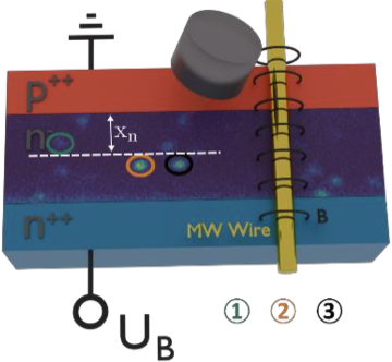
Quantum sensing based on color centers is a widely used quantum technology in various applications such as physics, biology, and engineering. It offers the possibility to precisely measure faint physical quantities like magnetic or electric fields at nanometer-scale resolution. Based on these capabilities, we investigated the complex interplay of charges and electric fields within an electronic device in 4H silicon carbide. Our results showed that quantum sensors can precisely monitor changes in charges, doping, and the evolution of the depletion zone during the operation of an electronic device with nanometer resolution, which was not experimentally accessible until now. These results will play an important role in the future development of new electronic devices and in monitoring electronic device physics.
For more information, see their publication in Physical Review Applied:
Quantum-enhanced electric field mapping within semiconductor devices
D. Scheller, F. Hrunski, J.H. Schwarberg, W. Knolle, Ö.O. Soykal, P. Udvarhelyi, P. Narang, H.B. Weber, M. Hollendonner, R. Nagy
Phys. Rev. Applied 24, 014036 (2025)